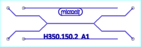
H-shaped channel for boundary flow experiment - 350 x 150µm

SKU
11003577
Availability:
check_circle In stock
$341.31

per pack of 3

H-shaped flow channel, ideal for boundary flow experiments.  The channels have a width of 350µm and height of 150µm.

This H-shaped flow channel is an ideal solution for boundary flow experiments in which two liquids will flow in parallel and only diffusion will occur at the interface of both flows. 

The channels are etched into borosilicate glass (D263 Eco) which creates extremely smooth channels which are fully transparent. 
The channels have a width of 350µm and height of 150µm.
The main channel has a length of 14.8mm, the inlet/outlet structures a length of 14.5mm

The channel profile is as follow:

The chip has a thickness of 1.8mm, the height above the channel is 950µm.
The height below the channel is 700µm.

More Information
Unit of measurementpack of 3
Interface typeTopconnect
Chip materialBorosilicate glass - D263
Chip thickness1.8mm
Number of inlets2
Number of outlets2
Channel Width350µm
Bottom thickness700µm bottom layer
CoatingNo coating (hydrophilic)
Customer Questions
How do I clean my chips?
One simple but very effective way to clean a microchip is to flush an alkaline solution through the channels. A solution of 1 M sodium hydroxide in water works well, but a lower concentration might also be sufficient. If traces of the cleaning solution remain inside the chip after cleaning, rinse with water or ammonia. Further, plastic parts should not be exposed to alkaline solutions.
To remove particulate matter from your chip, a water bath with ultrasonic agitation can be used, preferably while flushing a watery solution through the channels.
Glass microchips can be heated (e.g. 400°C) causing any organic material on the glass surface to degrade. Try to use lower temperatures first because burning the content could make it stick. Make sure you only heat the glass chip and not the plastic parts around it.
Concentrated sulfuric acid works well to dissolve organic material, such as fibres, that are difficult to remove with alkaline solutions. Always keep in mind that you are working with extremely corrosive material. Please note that this instruction is focused on the chip itself, PEEK elements like connectors are not so compatible with strong sulforic acid.
Please note that chips that were coated by Micronit have different guidelines for cleaning!
Can this flow cell be customized?
Absolutely! Micronit is a key supplier for flow cells in the Next Generation Sequencing market and can manufacture flow cells competely according to your specific requirements.  What can be customized?

The channel shape. The channel height and width.
For wet etching its important to consider that channel height and minimal channel width are related.
{minimal channel width} = 2 * {etch depth} + {initial mask opening, typcial 5-10µm} 
Larger aspect ratios (relation between channel depth and width) are possible using dry etching. For this, a glass/silicon combination is most common. Choice of material. For instance, fused silica is a good option when UV light is used. Schott D263 bio can be a good alternative for some specific fluorescent labels.  Surface flatness. We can provide ultra flat surfaces.
What is the roughness of the etched structures?
Wet etched structures are extremely smooth and have a roughness in Angstrom range. The structures are fully optical transparent. 
Large roughness for structures in glass chips is typical observed for structures manufactured by use of laser assisted manufacturing techniques or abrasion-based techniques like powder blasting. Almost all catalogue products from Micronit are manufactured using wet etching to create full transparent channels without substantial roughness. 
Would you like to submit a question? Please login first.
Copyright © 2020-present Micronit B.V. All rights reserved.