Cross channel chip

SKU
cross_channel
Availability:
check_circle In stock
As low as $295.62

per pack of 3

Pack of 3 cross channel chips.

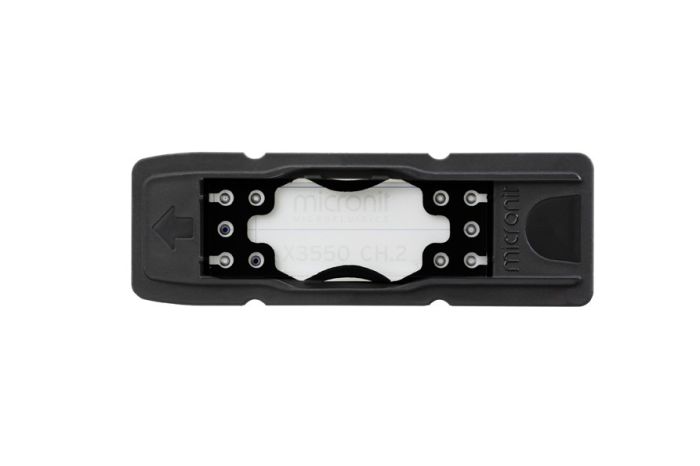
Microfluidic chip with two channels crossing each other. Also suitable for capillary electrophoresis (CE).

More Information
Unit of measurementpack of 3
Interface typeTopconnect
Chip materialBorosilicate glass
Number of inlets3
Number of outlets1
Channel width50
Icon Label Description Type Size Download
pdf X3550CH.3 - Drawing pdf 69.7 KB Download
Customer Questions
Can this flow cell be customized?
Absolutely! Micronit is a key supplier for flow cells in the Next Generation Sequencing market and can manufacture flow cells competely according to your specific requirements.  What can be customized? The channel shape. The channel height and width. For wet etching its important to consider that channel height and minimal channel width are related.{minimal channel width} = 2 * {etch depth} + {initial mask opening, typcial 5-10µm} Larger aspect ratios (relation between channel depth and width) are possible using dry etching. For this, a glass/silicon combination is most common. Choice of material. For instance, fused silica is a good option when UV light is used. Schott D263 bio can be a good alternative for some specific fluorescent labels.  Surface flatness. We can provide ultra flat surfaces.
When should I use the metal strips (spacers) as provided with the Fluidic Connect Pro holder?
When should I use the spacers?The metal strips are used for thin bottom chips and are also part of the holder for resealable flow cell's.This are currently the following products (list might be incomplete): SKU SKU old Description Note 11000746 00746 Fluidic Connect Pro for resealable flow cells Normally already pre-assembled  11000746 00745 Insert set for resealable flow cells   11003133 03133 Thin bottom flow cell    11106327 03133-F Thin bottom flow cell - coated   11003196 03196 Thin bottom flow cell - 0.5mm   11006345 03196-F Thin bottom flow cell - 0.5mm - coated   11003164 03164 Thin bottom flow cell - 1.5mm   11006338 03164-F Thin bottom flow cell - 1.5mm - coated   11003694 FC_R50.332.3_PACK Serpentine channel / Microreactor, 20x50µm, 342mm length   11003644 FC_R50.332.3-F Serpentine channel / Microreactor, 20x50µm, 342mm length - Coated   11003040 03040 Serpentine channel / Microreactor, 45x140µm, 350mm length     11006834 03040 - F Serpentine channel / Microreactor, 45x140µm, 350mm length - coated   11006722 FC_X3550CH.3_PACK Cross channel chip - thin bottom   How to apply the spacers? The spacers are placed beneath the top insert, as shown in the picture below. What should I do when I don't have spacers available?Just contact us to request new spacers.
What's important in selection of a suitable microscope objective?
An inverted microscope is recommended for observing flow in microfluidic chips, as most observation surfaces are located on the bottom (non-inlet) side. A key parameter in selecting a suitable objective is the working distance. For thin-bottom chips, the working distance is less critical, as the distance to the channel is typically below 175 µm. However, it is still recommended to minimize the size of the objective itself where possible, to allow more space for movement within the holder. For chips with regular (thicker) bottoms, the working distance becomes a critical factor. Most standard objectives are designed for use with a #1.5 cover slip, which has a thickness of only 170 µm. However, the bottom thickness of typical microfluidic chips is usually in the range of 400–900 µm. Therefore, long working distance objectives—often referred to as non-cover glass objectives—are more suitable. Whenever possible, we recommend using dry objectives, as they simplify the setup and eliminate the need for immersion media. In many cases, it is feasible to use the edge of the channel or another well-defined feature as a reference point for manual size correction. This approach can reduce the need for optical corrections provided by the objective itself.
What is the roughness of the etched structures?
Wet etched structures are extremely smooth and have a roughness in Angstrom range. The structures are fully optical transparent. Large roughness for structures in glass chips is typical observed for structures manufactured by use of laser assisted manufacturing techniques or abrasion-based techniques like powder blasting. Almost all catalogue products from Micronit are manufactured using wet etching to create full transparent channels without substantial roughness. 
Would you like to submit a question? Please login first.
Copyright © 2020-present Micronit B.V. All rights reserved.